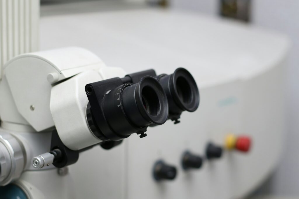
Scanning electron microscopy (SEM) is a revolutionary technique that allows for the acquisition of exceptionally precise images by studying the surface of samples at the microscopic scale. Used in numerous fields, it is distinguished by its ability to reveal morphological and chemical details invisible to the naked eye. In this article, we will explore the fundamental principles of this technology, its diverse applications, and its advantages for laboratory analysis.
1. Introduction
Introduction to scanning electron microscopy
Scanning electron microscopy, also known as SEM, is an advanced technique that uses an electron beam to analyze and image the surface of samples. Unlike traditional optical microscopes, SEM offers much higher resolution, allowing visualization of details on the order of nanometers.
Importance of SEM in laboratory analyses
SEM plays a vital role in modern laboratories. It allows for the characterization of the topography, morphology, and chemical composition of materials with unparalleled precision. This technique makes it possible to detect microscopic defects, control material quality, and gain a better understanding of the mechanisms behind failures in various systems.
Overview of application areas
SEM is widely used in many sectors, including industry, scientific research, medicine, and the environment. Whether for studying nanomaterials, analyzing particles, or characterizing surfaces, this technology has become indispensable for researchers and professionals seeking to solve complex problems.
2. Definition and principle of scanning electron microscopy
Description of operation
The scanning electron microscope uses a very fine electron beam to scan the surface of a sample point by point. During this scanning, the electrons interact with the material, producing different types of signals, including secondary electrons, backscattered electrons, and X-rays. These signals are then collected by detectors, allowing a detailed image of the surface to be reconstructed on a screen. This method offers unparalleled precision and depth of field, making it possible to explore samples at the nanoscale.
Types of emissions detected
When the electron beam strikes the surface of the sample, it generates several types of emissions:
- Secondary electrons: These originate from the outer shells of the sample's atoms and allow for the visualization of topographic details. These signals are used to produce images showing surface relief.
- Backscattered electrons: These electrons, reflected by matter, provide information on the chemical composition and density of the elements present.
- X-rays: Emitted during electron-matter interaction, they allow chemical analysis of the elements present in the sample, by coupling SEM with EDX spectrometry.
Comparison with traditional optical microscopes
Unlike optical microscopes, scanning electron microscopy (SEM) uses electrons instead of visible light, giving it a significantly higher resolving power. While the resolution limit of optical microscopes is around 200 nanometers, SEM can achieve resolutions on the order of nanometers. Furthermore, the depth of field of SEM is much greater, providing better visualization of three-dimensional structures.
Are you looking for an analysis?
3. Main applications of SEM in the laboratory
Surface and morphology analysis of materials
SEM is particularly effective for studying the topography and morphology of surfaces at the microscopic scale. It allows visualization of the reliefs, irregularities, and structures of different materials. These analyses are essential in fields such as engineering and materials science, where understanding the texture and surface properties of the objects under study is crucial.
Characterization of defects
SEM is an essential tool for detecting and analyzing defects on material surfaces. It allows for the identification of cracks, fractures, or areas of corrosion, providing precise information on the origin of these failures. This data is used to improve manufacturing processes or guarantee product quality.
Determination of elemental composition
Combined with energy-dispersive X-ray spectroscopy (EDX), SEM can determine the chemical composition of materials at the microscopic scale. This coupling makes it possible to locate and identify elements present on the surface of samples, a capability particularly useful for contaminant analysis, failure investigation, or the validation of industrial processes.
Study of nanomaterials and crystalline structures
SEM also plays a key role in the study of nanomaterials, such as nanoparticles and nanostructures. Thanks to its high resolution, it allows these structures to be analyzed with exceptional precision. Furthermore, by integrating technologies such as electron backscattering diffraction (EBSD), it is possible to characterize the crystallographic orientations and properties of microstructures.
4. Modern equipment and technologies
Types of scanning electron microscopes
There are several types of SEM, each designed to meet specific needs:
- Tungsten filament SEM : This type of SEM uses a heated filament to emit electrons. It is commonly used for general applications, offering adequate resolution for many analyses.
- Field-effect gun (FEG) SEM : Thanks to its more stable and concentrated electron source, this microscope achieves higher resolution, ideal for the analysis of nanomaterials and highly detailed structures.
- Environmental SEM (ESEM) : Designed to analyze non-conductive or hydrated samples, this type of microscope can operate under controlled pressure, thus avoiding invasive preparations such as metallization.
Technical specifications
Modern SEM equipment is distinguished by its advanced features:
- High resolution : Some models can achieve a resolution of 1 nanometer, allowing extremely fine visualization of samples.
- Extended depth of field : This feature allows for better visualization of three-dimensional structures, even on complex surfaces.
- Compatibility with various materials : Modern SEMs can analyze bulk, non-metallized or heat-sensitive samples, offering exceptional flexibility of use.
Recent innovations
Recent technological developments have transformed the SEM into an even more powerful tool:
- Digital SEM : These models incorporate digital control features and direct image scanning, facilitating processing and sharing.
- 3D imaging : Some SEMs are equipped with software that allows the reconstruction of three-dimensional images, ideal for analyzing topography in detail.
- Coupling with other techniques : SEM is often associated with technologies such as EBSD for crystallographic analysis or EDX for chemical composition, thus increasing its range of applications.
Accessibility and ease of use
Modern equipment includes ergonomic and technical improvements that make it easier to use:
- Automation of processes to reduce errors and analysis time.
- Intuitive user interfaces allowing for quick adoption by technicians and researchers.
5. Specific areas of application
Food industry
In the agri-food sector, SEM is an essential tool for guaranteeing product safety and quality. It is used for:
- Contaminant identification : Analysis of foreign particles such as metallic, plastic or organic fragments present in food.
- Quality control : Study of the structure of food to ensure compliance with manufacturing standards.
- Packaging analysis : Examination of packaging materials to detect possible interactions or migration of undesirable substances into food.
Industrial sector
In industry, SEM is used to optimize manufacturing processes and analyze failures. Its applications include:
- Fractographic expertise : Study of fracture surfaces to understand failure mechanisms in materials.
- Coating control : Analysis of thin layers applied to surfaces to assess their thickness, uniformity and adhesion.
- Study of corrosion phenomena : Identification of corrosion zones and underlying mechanisms to improve the durability of materials.
Medicine and biology
SEM is widely used in the fields of health and biomedical research. It allows:
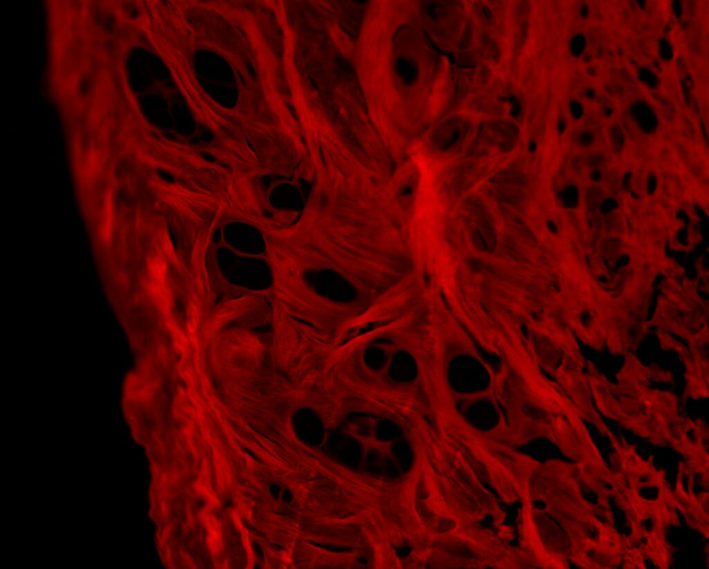
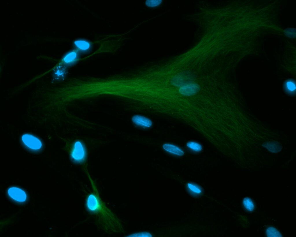
- Observation of biological tissues : Study of the morphology of cells and tissues to understand microscopic structures.
- Implant characterization : Analysis of materials used in implantology to guarantee their biocompatibility and resistance.
Environment
Within the field of environmental science, scanning electron microscopy (SEM) plays a key role in monitoring and preserving natural resources. Its applications include:
- Analysis of atmospheric particles : Study of pollutants present in the air to assess their impact on health and the environment.
- Soil examination : Observation of mineral and organic particles to understand their structure and composition.
- Water monitoring : Analysis of contaminants in water samples to assess their compliance with environmental standards.
Basic research
SEM is a cornerstone of scientific research, enabling the exploration of new properties and structures:
- Study of nanomaterials : Analysis of the properties and behavior of structures at the nanoscale.
- Characterization of new materials : Identification of structures and physical properties to develop innovative applications.
6. Advantages of SEM for laboratory analysis
High resolution and extended depth of field
SEM offers exceptional resolution, capable of capturing details on the order of nanometers. This precision allows the visualization of microscopic structures that would be invisible with other techniques. Furthermore, its large depth of field enables the acquisition of sharp images of complex three-dimensional surfaces, a major advantage for the analysis of irregular samples.
Flexibility in the choice of materials
One of the strengths of SEM is its ability to analyze a wide range of materials, whether metallic, organic, mineral, or composite. Thanks to innovations such as environmental microscopes, it is also possible to study non-conductive or hydrated samples without invasive preparation, further expanding its range of applications.
Combined information on morphology and composition
By combining SEM with technologies like EDX, it is possible to obtain morphological and chemical data simultaneously. This dual analysis is particularly valuable for applications such as contaminant identification, thin film studies, and failure characterization.
Reduction in sample preparation requirements
Unlike some techniques requiring complex preparation, SEM allows for the analysis of bulk or minimally modified samples, thus reducing the risk of degradation or alteration of results. Technological advances, such as variable pressure, also eliminate the need to metallize certain types of samples.
Detailed and actionable visual reports
The images produced by the SEM are exceptionally clear and can be used directly for in-depth analysis or presentations. The ability to produce 3D images adds another dimension to data interpretation, thus facilitating informed decision-making.
Compatibility with other analytical techniques
SEM can be integrated into a broader analytical workflow, complementing other technologies such as EBSD for crystallographic analysis or spectrometry for chemical characterization. This compatibility enhances its usefulness in projects requiring multidisciplinary approaches.
7. Coupling of SEM with other analytical techniques
Energy-dispersive X-ray (EDX) microanalysis
Coupling SEM with EDX provides detailed information on the chemical composition of samples. This detector measures the X-rays emitted when the electron beam interacts with matter. Each chemical element produces a unique spectrum, allowing:
- Identification of the elements present : A semi-quantitative analysis can be carried out to determine the relative proportion of the elements.
- Analysis of specific areas : The beam can be focused on inclusions or defects to understand their precise chemical composition.
This technique is particularly useful for coating analysis, contamination characterization, and the study of composite materials.
Electron backscattered diffraction (EBSD)
EBSD, often used in conjunction with SEM, allows for the analysis of the crystallographic properties of materials. It relies on the diffraction of backscattered electrons as they interact with a crystalline surface. Its applications include:
- Characterization of crystallographic orientations : This analysis is essential for understanding the mechanical and thermal properties of materials.
- The study of microstructures : It allows the identification of grains, grain boundaries and textures in metals and ceramics.
EBSD is particularly valued in the metallurgical industry and for the development of new materials.
Coupling with 3D imaging
Modern SEMs integrate 3D imaging software, enabling the reconstruction of three-dimensional models of surfaces. This coupling is useful for:
- Visualizing complex structures : Three-dimensional analysis allows us to examine geometries that are difficult to access with a flat image.
- Measuring volumes and reliefs : This data is essential for studies on the porosity or density of materials.
Synergy with other spectroscopic techniques
In the laboratory, SEM can also be integrated into a broader analytical workflow, combined with techniques such as:
- Infrared (IR) spectroscopy : For the analysis of chemical bonds and functional groups.
- Gas chromatography coupled with mass spectrometry (GC-MS) : For the identification of volatile organic compounds present on the analyzed surfaces.
8. Constraints and limitations of the technique
High cost of equipment and maintenance
Scanning electron microscopes are cutting-edge tools, which translates into a high acquisition cost. Added to this are significant expenses for regular maintenance, which includes:
- Checking electronic components : The electron gun and detectors require precise maintenance to guarantee their performance.
- Replacing consumables : Some parts, such as tungsten filaments, have a limited lifespan and must be replaced periodically.
These costs can limit access to SEM, particularly for small laboratories or businesses.
Specific preparation of samples
Although SEM allows the analysis of a wide variety of materials, some samples require complex preparation:
- Sample metallization : Non-conductive materials often need to be coated with a thin layer of metal (gold, palladium) to avoid charging effects, which can alter certain characteristics.
- Vacuum conditions : Samples must be compatible with the high vacuum conditions required by the SEM, excluding materials containing water or volatile solvents without prior preparation.
These constraints lengthen the delays and may introduce changes to the sample.
Limitations related to the nature of the materials
SEM can encounter difficulties with certain materials:
- Fragile materials : Sensitive samples can be damaged by the electron beam, especially during prolonged or high-energy analyses.
- Limited resolution for very large samples : Massive or complex samples may require specific adjustments for optimal analysis.
Data interpretation
Although SEM provides highly accurate images and spectra, their interpretation requires advanced technical expertise:
- EDX spectrum analysis : X microanalysis results must be carefully interpreted to avoid errors due to peak overlaps.
- Image complexity : Topographic and chemical contrasts may require extensive training to draw reliable conclusions.
Energy consumption and environmental impact
Electron microscopes consume a significant amount of energy, which can be a concern from a sustainability perspective. Furthermore, some consumables (inert gases, precious metals for metallization) have a considerable environmental impact.
The limitations associated with SEM, while significant, do not diminish its value as an analytical tool. With continuous technological advancements and specialized training, these limitations can be mitigated, making this technique even more accessible and effective.