SEM EDX (Scanning Electron Microscopy coupled with Energy Dispersive X-ray Analysis) is an essential technique in materials analysis.
Combining morphological observation and chemical analysis, it allows for the precise characterization of the surface of a sample, while identifying the elements that compose it.
Used in many sectors such as metallurgy, biology, nanotechnology, or the field of nutraceuticals , and many others, this method offers unparalleled resolution for the study of microscopic structures.
This article explores in depth the principles of SEM-EDX, its advantages, and its industrial and scientific applications.
1. What is a Scanning Electron Microscope (SEM)?
The Scanning Electron Microscope (SEM) is a revolutionary tool that allows observation of a sample's surface at a microscopic scale using an electron beam. Unlike an optical microscope, which uses photons (light particles), the SEM uses electrons to interact with matter, resulting in images with significantly higher resolution.
How does a SEM work?
The SEM works by projecting a beam of electrons onto the surface of a sample. This beam scans the surface point by point, generating various interactions with the material. Among these interactions, two main types of emitted electrons are distinguished: secondary electrons and backscattered electrons .
- Secondary electrons : These are used to image the sample surface, providing strong topographic contrast . These low-energy electrons are ejected from the sample during interaction with incident electrons. They allow visualization of fine surface details, such as roughness, micro-cracks, and other morphological features.
- Backscattered electrons : These electrons are used to create chemical contrast . They are more energetic than secondary electrons and are reflected by matter depending on its chemical composition. Heavier materials, such as metals, appear lighter in the image, while lighter materials appear darker.
By scanning the sample with the electron beam, the SEM allows for the reconstruction of a high-resolution image of the observed object's surface. This makes it an essential tool for researchers and engineers who need to visualize structures at the nanoscale.
Types of SEM imaging
The SEM offers several imaging modes depending on the detectors used and the types of interactions analyzed:
- Secondary electron (SE) imaging : This mode allows visualization of the sample topography. It is particularly well-suited for studying surface defects, fractures, and rough structures.
- Backscattered electron imaging (BSE) : This mode is ideal for identifying differences in chemical composition within a sample. It is widely used in the analysis of metals, alloys, and other heterogeneous materials.
These different imaging modes make it possible to adapt observations according to the specific needs of each analysis project, whether for the study of the surface of a material or for the differentiation of the chemical elements present.
2. What is the difference between SEM and TEM?
Scanning Electron Microscope (SEM) and Transmission Electron Microscope (TEM) are often used in a complementary manner, but they offer very different analytical approaches.
SEM: Surface observation
SEM surface observation technique where an electron beam scans the surface of a sample, generating interactions that allow for the reconstruction of a topographic image. SEM is particularly effective for examining surface defects , microscopic textures, and phenomena such as corrosion and microcracks. Thanks to its large depth of field, it allows for the observation of relatively large samples without requiring complex preparation.
The advantages of SEM include:
- Non-destructive surface analysis.
- The ability to examine massive samples without complex preparation.
- A large depth of field for a clear visualization of the surface.
MET: Internal Analysis of Structures
TEM the other hand, is used to observe the interior of samples , often at an even finer scale than SEM. In this technique, the electron beam passes through the sample, allowing images of internal structures to be obtained at atomic resolution . This is particularly useful for studying the crystalline structure of materials, as well as for observing internal details of cells or nanoparticles.
The advantages of the MET include:
- Extremely high resolution, often at the atomic scale.
- Observation of the internal structures of the sample, including cells or nanoparticles.
However, TEM requires more rigorous sample preparation. Samples must be extremely thin (often on the order of a few nanometers thick) to allow electrons to pass through them, which limits its use to fragile materials or complex structures. Furthermore, unlike SEM, TEM does not allow observation of samples in 3D, as the image obtained is generally a two-dimensional projection.
Specific applications of SEM and TEM
The differences between SEM and TEM make them useful in different contexts.
- SEM is widely used in industries to analyze bulk materials, surface defects, and wear phenomena, making it indispensable in sectors such as metallurgy, electronics, and materials science.
- MET , on the other hand, is mainly used in research for fundamental studies of atomic structures, particularly in molecular biology, nanotechnology, and crystallography.
Thus, the choice between SEM and TEM depends on the needs of the study: SEM excels in surface observation and 3D analysis, while TEM is ideal for the internal examination of fine structures with atomic resolution.

3. What is the SEM in Life and Earth Sciences?
In the field of Earth and Life Sciences , scanning electron microscopy (SEM) is a valuable tool for studying the morphology and composition of biological, geological, and paleontological samples. Its use allows for the acquisition of high-resolution images of microscopic structures, whether plant cells, fossilized insects, or microminerals.
Use of SEM in biology
SEM cellular and tissue structures of the surface of cells and organisms, offering a deeper understanding of their organization.
- Observation of plant and animal cells : Thanks to SEM, it is possible to observe the external structures of plant cells (cell walls, stomata) and animal cells (cell membranes, microvilli). These images allow for a better understanding of their function and organization.
- Study of microscopic organisms : SEM is particularly useful for analyzing microscopic organisms, such as bacteria, viruses, or fungi, by visualizing their surface structure with a resolution far superior to that of an optical microscope.
Use of SEM in geology
In geology , scanning electron microscopy (SEM) is used to study minerals , rocks , and fossils . It allows geologists and paleontologists to analyze the microscopic structures of samples and to better understand their formation and composition.
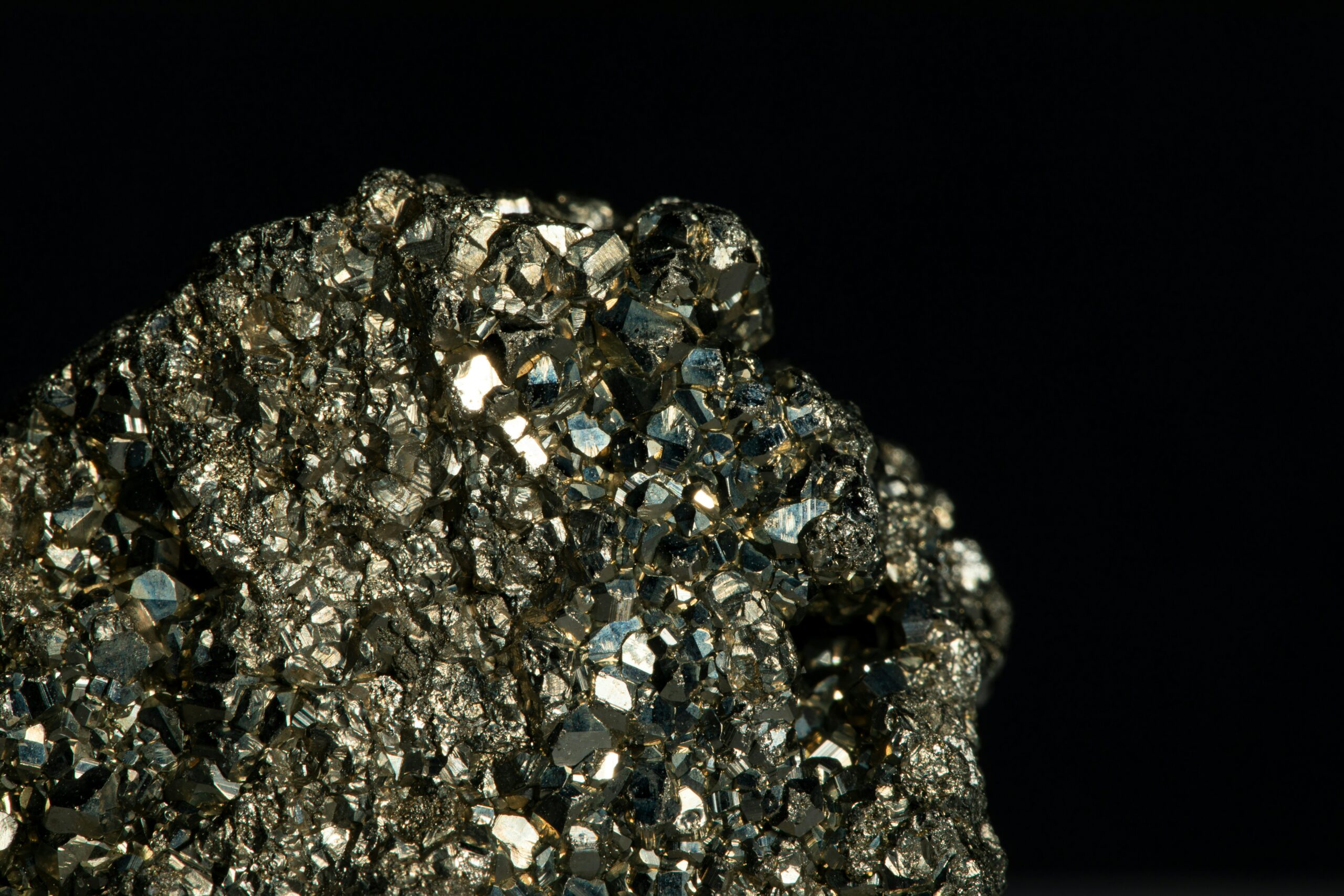
- Mineral and rock analysis : SEM allows observation of the surface of minerals and rocks, revealing details about their formation, chemical composition, and alteration over time.
- Studying fossils : Paleontologists use SEM to study fossils at a microscopic scale. It reveals features such as the structure of fossilized bones, the texture of skin or feathers, and even details about the preservation of the fossils.
Advantages of SEM in Life and Earth Sciences
The SEM offers several advantages for researchers in life and earth sciences :
- High resolution : Allows observation of details invisible to an optical microscope.
- Non-destructive analysis : The samples are not altered by the analysis, which allows them to be reused for other tests.
- Adaptability : SEM can be used on a wide variety of materials, from biological samples to minerals and fossils.
Thanks to its ability to provide high-resolution images and analyze the chemical composition of samples, SEM is an indispensable tool for scientists working in the field of Life and Earth Sciences , offering new perspectives in the study of biological and geological microstructures.
4. Coupling of SEM with EDX for chemical analysis
The coupling of SEM and EDX of visual surface analysis of a sample with information on its elemental composition. This method is particularly effective for complex materials, alloys, and minerals, where it is crucial to know not only the shape but also the exact chemical composition of each part of the sample.
How the EDX works
Energy Dispersive X-ray Spectroscopy (EDX) works by analyzing the X-rays emitted by atoms in the sample when they are bombarded by electrons from the SEM beam. When the electrons strike the sample, they excite the atoms, causing the emission of X-rays characteristic of each chemical element present. These X-rays are then captured by the EDX detector, which converts the data into an energy spectrum. Each energy peak chemical composition of the analyzed area to be determined
Semi-quantitative and qualitative analysis
EDX allows for both qualitative (identification of elements present) and semi-quantitative (approximate measurement of element concentrations) analyses. However, quantitative accuracy is limited by factors such as electron penetration depth, sample geometry, and analysis conditions. Despite this, the technique is extremely useful for obtaining rapid and reliable information on the elemental composition of materials.
Applications of SEM-EDX coupling
The SEM-EDX is used in a wide range of industrial and scientific applications:
- Analysis of metallic materials : In metallurgy, SEM-EDX allows the study of alloys and corrosion phenomena, by identifying the chemical elements responsible for surface degradation.
- Mineral characterization : In the mining and geological industries, SEM-EDX is used to identify the elements present in rocks and ores, thus facilitating the exploration of natural resources.
- Micro-defect analysis : In the manufacture of electronic components and printed circuit boards, SEM-EDX helps to identify contaminants or chemical defects that may affect the performance of the final product.
- Nanotechnologies : In the study of nanomaterials, SEM-EDX allows for the analysis of the chemical composition of nanostructures with exceptional precision, thus helping to improve the performance and stability of these materials.
Advantages of SEM-EDX coupling
- Simultaneous morphological and chemical observation : SEM allows for high-resolution images, while EDX provides information on the elemental composition of the surface, thus offering a complete understanding of the sample.
- Non-destructive analysis : This method preserves the integrity of the sample while obtaining precise information on its chemical composition.
- Versatility : The MEB-EDX can be used on a wide range of materials, from metals to ceramics, polymers and biological samples.
In summary, coupling SEM with EDX allows us to go beyond simply observing the surface of a sample, providing precise data on its chemical composition. This approach is particularly valuable in fields where detailed analysis is required, such as the metallurgical industry, materials research, or the manufacturing of electronic devices.
5. Why does the SEM operate under vacuum?
The operation of the SEM requires an environment where air particles are virtually absent. This vacuum is essential for several reasons related to image quality, measurement accuracy, and the protection of the analytical equipment.
No interference with air molecules
When the electron beam is emitted by the microscope's electron gun, it must travel a direct path to the sample. If air molecules (oxygen, nitrogen, water vapor, etc.) are present in this path, they will collide with the electrons , thus scattering the beam. This phenomenon, called elastic and inelastic , impairs the precision of observations and reduces the quality of the resulting image.
Placing the sample in a vacuum chamber minimizes these interferences, ensuring better focusing of the electron beam and clearer, more precise imaging. This results in much higher resolutions and better image quality.
Sample preservation
Some samples, particularly those containing organic or hydrated components, can undergo chemical or physical when exposed to electrons in an atmosphere containing air or moisture. A vacuum protects these samples from reactions with oxygen or other molecules present in the air, thus ensuring better preservation of the sample's initial properties during analysis.
Furthermore, the absence of gas molecules prevents the charging phenomenon that can occur on non-conductive materials. In a vacuum environment, these charges are dispersed more uniformly, thus avoiding artifacts in the resulting image.
The different types of vacuum in SEMs
All SEMs operate under vacuum, but some allow working with different vacuum levels depending on the needs of the sample.
- High vacuum SEM : This is the most common option for obtaining high-resolution images. The vacuum in the sample chamber is pushed to very low levels (extremely low pressure), which is ideal for solid and conductive materials.
- Variable pressure SEM : This type of microscope allows the vacuum level in the sample chamber to be adjusted. It is particularly useful for analyzing non-conductive materials or samples sensitive to dehydration, such as biological or organic samples. This system allows a small amount of gas (usually water vapor or argon) to be introduced into the chamber to prevent electron charging of non-metallic samples.
Advantages of Variable Pressure SEM
Variable pressure scanning electron microscopy (SEM) allows the observation of samples that would not tolerate a complete vacuum environment. This offers several advantages:
- Non-conductive samples : In traditional high-vacuum microscopes, non-conductive samples often need to be coated with a thin metallic layer (metallization) to prevent electrostatic charges. With a variable-pressure SEM, this metallization can be avoided, as the low-pressure environment neutralizes the charges on the samples while maintaining good image quality.
- Observation of biological samples : Biological materials, often rich in water, can be observed without metallization and without complete dehydration. This preserves the natural properties of the sample while allowing for a detailed morphological analysis.
The challenges of vacuum in the SEM
While a vacuum is crucial for the proper functioning of the SEM, it also presents certain challenges. Fragile or dehydration-sensitive samples must be carefully prepared before being placed in the vacuum chamber. This may include drying or freezing techniques (such as using a Peltier plate to observe samples at -30°C) to preserve their structure and prevent alteration during analysis.
In summary, the use of vacuum in SEM is a technical necessity to guarantee the quality of the images obtained and to preserve the integrity of the samples. Although this constraint may impose limitations on certain types of samples, solutions such as variable pressure SEM now make it possible to overcome these obstacles, paving the way for a broader and more precise analysis of different materials.
Are you looking for an analysis?
6. Advantages of the SEM-EDX technique
SEM -EDX combines the strengths of two complementary methods: high-resolution imaging by Scanning Electron Microscopy (SEM) and chemical analysis by Energy Dispersion Spectrometry (EDX). This combination offers numerous advantages for observing and analyzing the morphology and chemical composition of materials.
1. Simultaneous morphological and chemical observation
One of the main advantages of SEM-EDX is its ability to provide morphological and chemical about the sample in a single analysis. While SEM allows observation of the sample surface at very high resolution, EDX provides a precise analysis of the elements present on that surface. This dual approach allows researchers to:
- Visualize microscopic structures (fractures, porosity, roughness) while identifying the nature of the chemical elements present.
- Mapping the chemical composition of specific areas of a sample, revealing variations in elements within micro-regions.
2. Non-destructive analysis
The SEM-EDX technique is often described as non-destructive because it does not require cutting or destroying the sample to obtain information. This is particularly important for valuable or rare samples, such as fossils, works of art, or complex electronic components, which must remain intact after analysis.
3. Wide range of analyzable samples
The SEM-EDX can be used to study a wide variety of materials, including metals , ceramics , polymers , and even biological materials . The SEM's ability to operate in vacuum or variable pressure environments allows for the observation of non-metallic samples while minimizing preparation (metallization, dehydration).
Typical sample types analyzed include:
- Metals and alloys : for studies on corrosion, heat treatments, or inclusions of foreign elements.
- Biological materials : cells, tissues, living or fossilized microscopic structures.
- Polymers and composites : for the characterization of the structure and the distribution of additives.
4. High resolution and depth of field
SEM of structures at the nanoscale. Furthermore, SEM provides a depth of field , allowing for sharp images of irregular and complex surfaces. This is crucial for studies of materials with complex topographies, such as powders, composites, or damaged surfaces.
7. Limitations of the SEM-EDX technique
Despite its many advantages, the MEB-EDX also has some limitations that can pose technical or practical challenges for certain applications.
1. Need for a vacuum environment
( SEM) requires a vacuum environment to operate, which can be problematic for samples sensitive to dehydration , such as organic materials or biological samples. Although variable-pressure SEMs exist to allow observation without metallization, certain vacuum-related constraints remain a limitation, particularly for hydrated or volatile samples.
2. Sample conductivity
Another challenge of electron microscopy is the need for samples to be conductive . Non-conductive materials, such as polymers , often need to be coated with a thin metallic layer (usually gold or carbon) to prevent the buildup of electron charges, which can lead to image distortion. This preparation step can sometimes alter the sample surface, making a completely accurate analysis difficult.
3. Limits of the depth of chemical analysis
EDX analysis is primarily limited to the surface . Due to the shallow penetration of electrons, chemical analysis is essentially performed to a depth of a few micrometers. This means that SEM-EDX is not suitable for in-depth analysis of bulk materials or for internal composition studies at great depths.
4. Accuracy of semi-quantitative analysis
Although EDX can determine the chemical composition of samples, the method remains semi-quantitative . The accuracy of the results can be affected by factors such as sample thickness, surface inclination, or interference between neighboring elements. Thus, while chemical trends can be clearly identified, the quantitative results should be interpreted with caution and compared to other analytical methods for more precise measurements.
8. Industrial applications of SEM-EDX
SEM -EDX has become an indispensable tool in several industries. It allows for quality control analyses , the identification of defects, and the optimization of manufacturing processes in numerous fields.
1. Metallurgy and materials
In the metallurgical industry, SEM-EDX is widely used to analyze the structure of alloys and identify defects related to production or material wear. It allows visualization of fractures, microcracks, and corrosion damage, while also providing information on the chemical composition of the various elements involved.
- Alloy analysis : SEM-EDX helps study the distribution of chemical elements in alloys and identify areas where chemical segregation may occur. This allows engineers to understand how to improve the strength and durability of materials used in metallic structures.
- Corrosion studies : SEM-EDX is also crucial for analyzing corrosion processes in industrial environments. By identifying the chemical elements responsible for degradation, companies can better predict and prevent corrosion, thus optimizing the lifespan of their products.
2. Microelectronics and Semiconductors
In the semiconductor and electronics component industry, SEM-EDX is used to analyze the structure and composition of printed circuit boards , chips , and microsystems . It allows the detection of defects such as the presence of foreign particles , contamination layers , or anomalies in manufacturing processes.
- Contaminant identification : One critical application is the detection of contaminating particles on electronic circuits, which can impair device operation. SEM-EDX not only allows visualization of these particles but also the determination of their chemical composition, enabling tracing their origin and improving manufacturing processes.
- Quality control of solder joints : The MEB-EDX is also used to check the quality of solder joints on printed circuit boards and to ensure that no failure leads to a malfunction of the electronic system.
3. Materials Science
SEM -EDX plays a key role in the field of materials science , where it is used to study the structure of composite materials , ceramics , and polymers . It allows for the characterization of interfaces, porosities, and charge distribution within materials.
- Ceramic and polymer studies : SEM-EDX enables detailed analysis of materials used in the aerospace, automotive, and medical industries, identifying structural or chemical composition defects. This contributes to the improvement of materials used for critical components, such as parts resistant to high temperatures or wear.